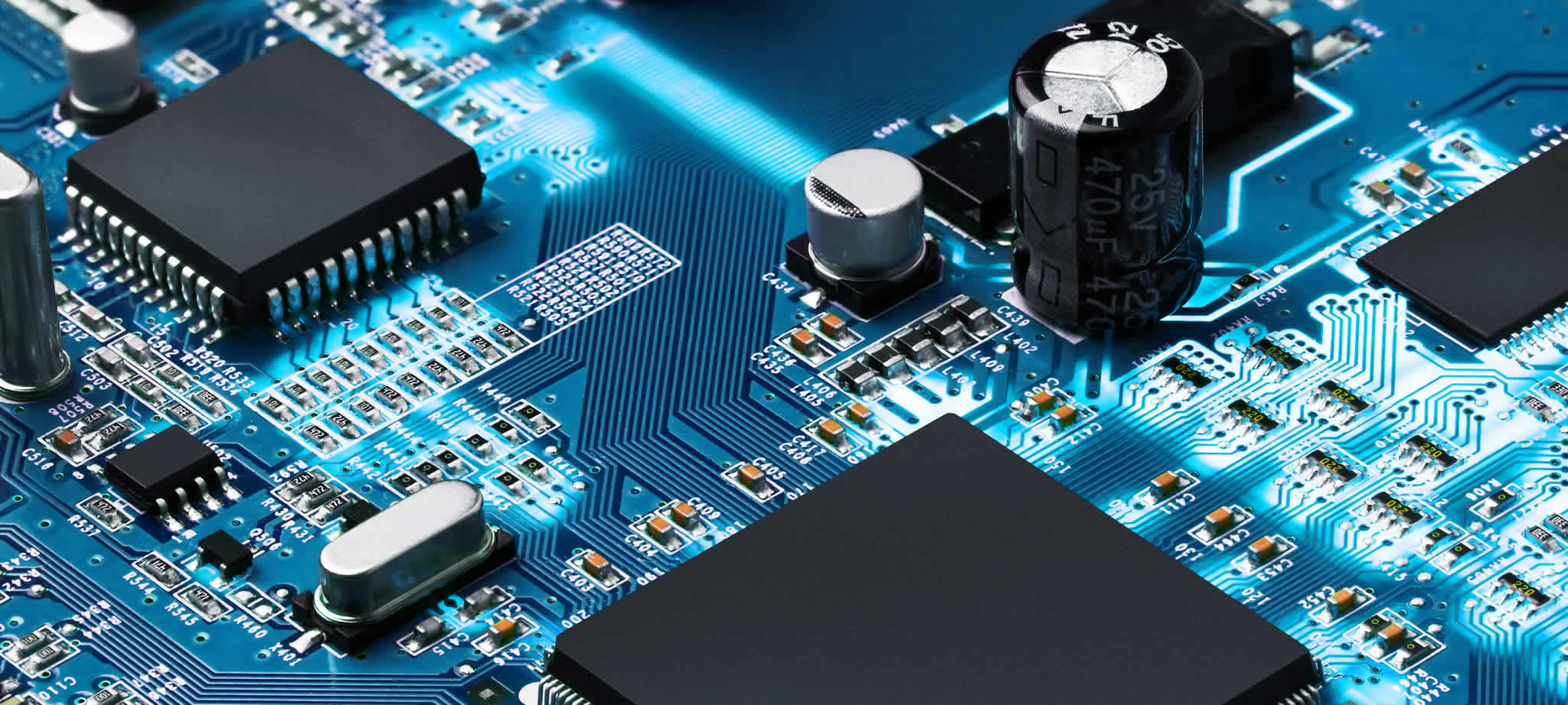
In the consumer electronics industry, semiconductor assembly and testing services assist manufacturers create semiconductors, memory chips, and wafers used in consumer electronics and wireless/mobile devices more efficiently.
Continuous developments and implementation of new technologies in the semiconductor assembly and testing services market, such as organic-substrate-interposer technology and silicon-via-interconnection technology, are creating significant revenue opportunities for players in the semiconductor assembly and testing services market.
In the consumer electronics industry, semiconductor assembly and testing services assist manufacturers create semiconductors, memory chips, and wafers used in consumer electronics and wireless/mobile devices more efficiently.
During the projected period of 2019-2029, the worldwide semiconductor assembly and testing services market is expected to grow at a CAGR of 5.8%.
Key Takeaways of Semiconductor Assembly and Testing Services Market Study
Request a Sample of this Report:
https://www.futuremarketinsights.com/reports/sample/rep-gb-2561
Gains Upheld by Increasing Demand for Improved Connectivity in Consumer Electronics
Higher demand for mobile and connected devices such as tablets and smartphones, has bolstered the demand for higher packaging technologies. Also, rising demand for digital video content drives growth of high performance and mobile consumer electronics products, such as Wi-Fi chipsets and other semiconductor chips. For instance, STATS chipPAC (JCET) develops expanded Wafer Level Chip Scale Package (eWLCSP), which offers improved testing and a low cost fan-in wafer level package for space-controlled mobile devices.
Moreover, growth of end-use industries such as electronics and semiconductors, automotive, manufacturing, and packaging is expected to offer potential growth opportunities for manufacturers in the global semiconductor assembly and testing services market.
ODMs and OEMS to Prioritize ‘Fab-lite’ Strategy
As semiconductor process technology migrates to larger wafers and smaller feature sizes, cost of building state-of-the-art wafer fabrication factories has risen significantly, reaching several billion dollars. High investment costs for next generation silicon technology and equipment are influencing various semiconductor companies to adopt or maintain a ‘fabless’ or ‘fab-lite’ strategy. The increasing demand for semiconductors are needed for cloud integration and connectivity with including sensors, computing, interactivity and communication devices.
Ask An Analyst:
https://www.futuremarketinsights.com/ask-the-analyst/rep-gb-2561
More Valuable Insights on Semiconductor Assembly and Testing Services Market
FMI’s report on the semiconductor assembly and testing services market is segmented into three major sections such as services (assembly & packaging services (copper wire & gold wire bonding, flip chip, wafer level packaging, TSV, others), and testing services), applications (communications, computing & networking, consumer electronics, industrial and automotive electronics, and region to help readers understand and lucrative evaluate opportunities in the semiconductor assembly and testing services market.
Future Market Insights (ESOMAR certified market research organization and a member of Greater New York Chamber of Commerce) provides in-depth insights into governing factors elevating the demand in the market.
Jul 19, 2022


Copyright © 2006 - 2023 PRnob Media, UBIC Solutions, LLC. All Rights Reserved.
